

Modern Electronic Hardware Design: An overview
Date: June 26, 2024
Electronic hardware is found in a wide range of products, from consumer gadgets to industrial equipment. The market success of these products often depends on how well their hardware performs. However, designing hardware is inherently complex— involving multiple stages with unique challenges and requirements. At Beta Solutions, with over 16 years of experience, we have developed a process that helps manage these complexities. This blog aims to provide a high-level overview of some of this process, highlighting the first three distinct phases. While developing these products successfully entails hardware, mechanical and firmware development, this blog will focus specifically on electronic hardware design.
The Beta Solutions Hardware Design Flow
The following process has been refined over time and is now used for the majority of our product development projects. However, it's worth mentioning that some projects demand a more “agile” methodology due to their unique needs and constraints. Agile hardware design will be a topic we tackle in a future blog.
While these phases appear linear on paper (known as a Waterfall model), keep in mind that in reality, each stage involves multiple iterations, and some stages may run concurrently.

Phase 0 - Pre-engagement Evaluation
In this initial phase, we hear about our clients' initial requirements, discuss how Beta Solutions can assist with their development, and discuss what the R&D journey might look like. We also address aspects like intellectual property, sales projections, and provide ballpark estimates for the possible investment and timeframes involved.
The project will formally kick off once the prospective client has approved both our Letter of Engagement and our Phase 1 proposal.

Phase 1 - Discovery & Specification
The objective of Phase 1 is to scope the project work, providing a strong foundation for the remainder of the product development process.
Core Outcomes/Tasks:
- Understand: Gaining insight is crucial for informed design decisions. Focus areas include:
- Customer: Gain insights into the client's needs, objectives, and pain points.
- Market: Analyze the industry landscape to identify risks, challenges, and opportunities.
- End User: Understand the target demographics and user behaviours to ensure the product meets user expectations and requirements.
- Compliance: Evaluate what regulatory compliance standards the project must meet - including electromagnetic compatibility (EMC) requirements.
- Risk Analysis: Assess potential project risks and ways to mitigate them.
- Hardware Features: Define what hardware features are needed in this product.
- Electrical Specifications: Develop reasonably comprehensive specifications that outline the design requirements and goals.
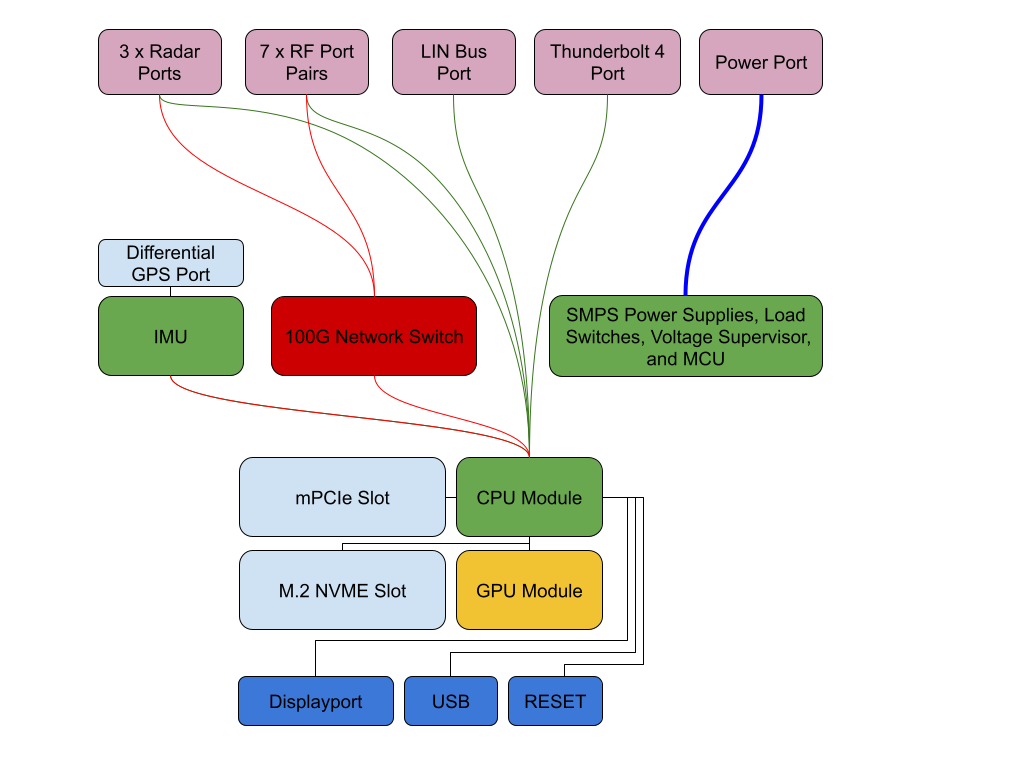
- Architecture: Develop a high-level system architecture outlining the interconnections between major features and subsystems.
- Select Key Components: Identify and choose specific components that will form the core of the product.
- Production Estimates: Provide a ballpark estimate for manufacturing costs. These estimates are based on initial assumptions and are just that, an estimate.
All of the above are defined in a “Project Discovery Report.” This report summarises the findings from Phase 1, confirming that there are sufficient specifications and a solid foundation to advance to the next phase.
When Is Phase 1 Finished?
Phase 1 is completed when the client approves the Project Discovery & Specifications Report. This approval confirms that the project's foundation is solid and that all critical specifications have been identified.
Subsequently, a proposal outlining the remaining work to be undertaken and the estimated investment required will be presented to the client. The move to Phase 2 is initiated once the client approves this new proposal.
Phase 2 - Detailed Design & Testing
The objective of Phase 2 is to meticulously refine and engineer the product into reality. This is where the bulk of the detailed work is undertaken.
Phase 2 of hardware design can be broadly split into three main sections:
- Schematic Design.
- PCB Placement & Routing.
- Prototyping & Testing.
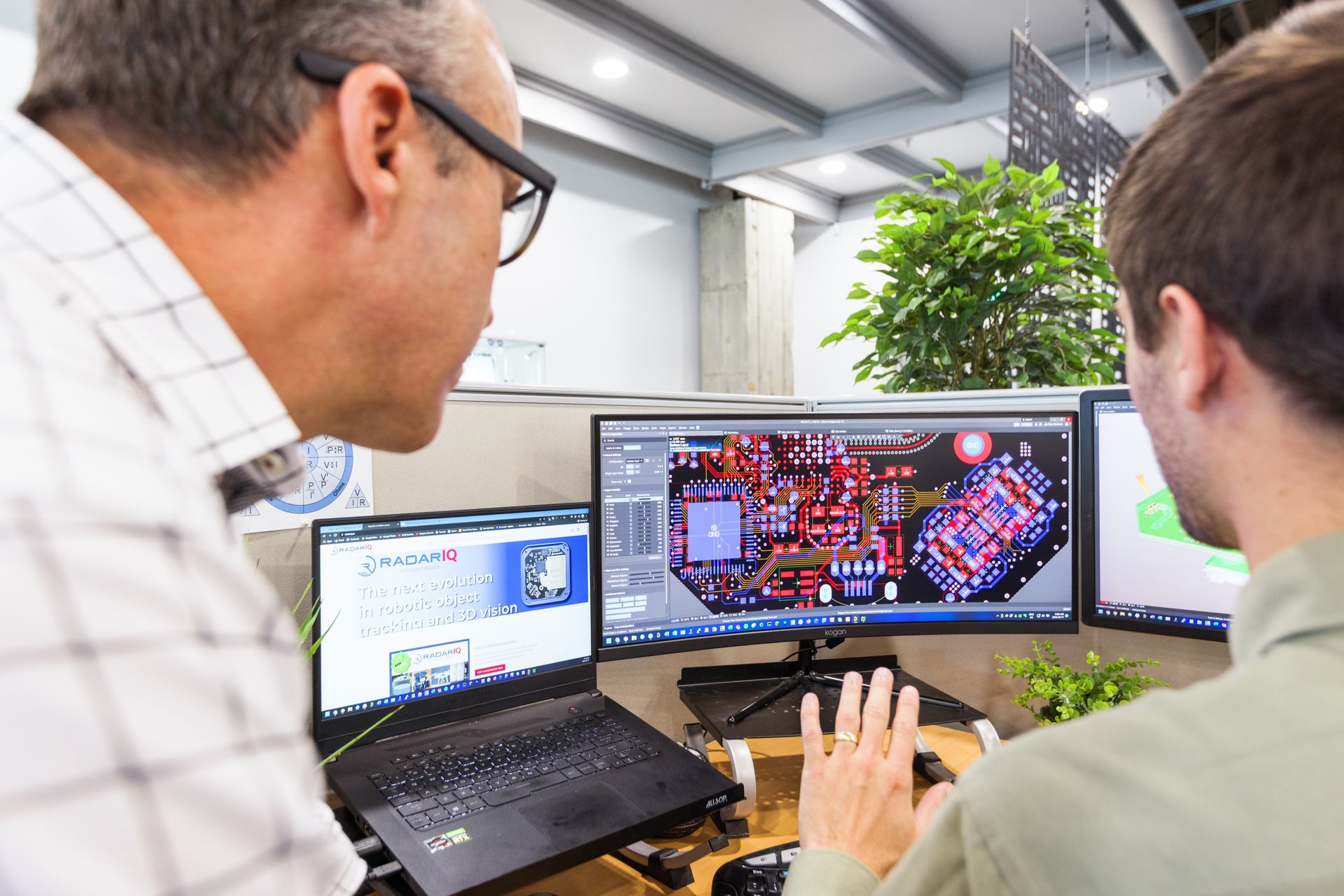
Schematic Design
What is a Schematic?
A Schematic is a detailed graphical representation of the product's electronic circuitry. It serves as a blueprint, showing which components are interconnected to which.
What makes Schematic Design Complex?
Schematic design is inherently complex due to the need for a deep understanding of every component. This complexity is further compounded by the necessity to consider how each component interacts with all the other connected components.
Core Outcomes/Tasks:
NB: While the tasks listed below cover some of the key aspects and outcomes essential to the schematic design phase, they are by no means exhaustive.
- Component Selection: Finalize the selection of each component, ensuring they meet the design requirements and constraints. This task involves reviewing datasheets to understand the properties and capabilities of each component. Each component will have tradeoffs to consider including:
- Performance.
- Size.
- Cost /Availability.
- Component Interconnection: Connect the selected components in the schematic.
- Documentation: A finished schematic will be populated with copious notes from the hardware engineer for several reasons:
- Design calculations.
- Key design decisions.
- Instructions for firmware engineers.
- Circuit Simulation: Perform circuit simulations to validate the design before physical prototypes are made. This involves using software tools like
LT Spice to simulate the behaviour of the circuit, allowing for the identification and resolution of issues in a virtual environment.
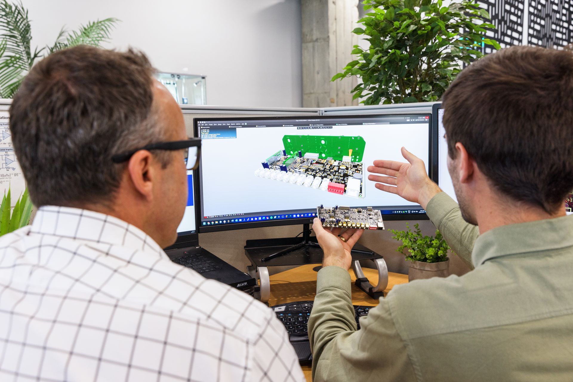
- Peer Reviews: Throughout the schematic design process, the design is reviewed multiple times by multiple people, including senior hardware engineers and firmware engineers working on the firmware aspects of the project. Additionally, an architecture review is conducted to ensure that the overall system design aligns with the initial specifications in phase 1.
During this phase, we continue to collaborate with the client to ensure that the design remains on track and aligned with the client's requirements.
PCB Placement & Routing
What is a PCB?
A Printed Circuit Board (PCB) is the physical board that hosts the components and connections illustrated in the schematic.
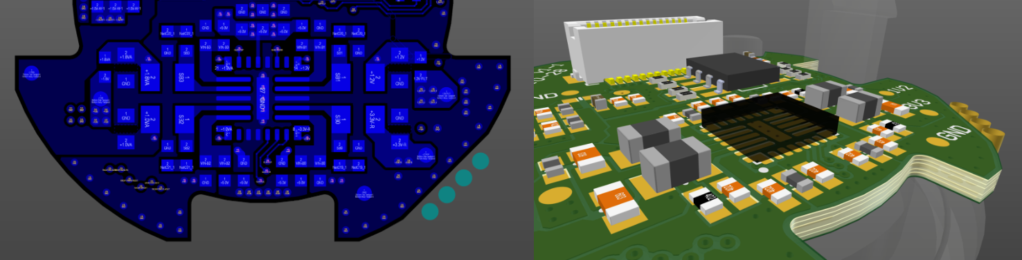
What is PCB Placement and Routing?
PCB Placement & Routing involves arranging the electronic components on the physical board and creating the conductive pathways (traces) that connect these components.
What Makes PCB Placement & Routing Complex?
PCB Placement & Routing is inherently complex due to multiple factors:
- Electromechanical Considerations: Collaborating with mechanical engineers (internal or external) to ensure that the initial layout of key components fits within the product’s physical constraints.
- Signal Integrity: Ensuring that signals are transmitted without interference or degradation. This is particularly important for any high-frequency signals.
- Thermal Management: Managing heat dissipation to prevent overheating.
- Manufacturability: Depending on where the PCBs are intended to be manufactured, they will need to meet specific design rules and constraints set by the manufacturing facility. These rules can include minimum trace widths, spacing, number of layers, and other parameters that ensure the boards can be produced using the equipment and processes available at the facility.
- Electromagnetic Compatibility (EMC) Considerations: This involves both minimizing the emissions generated by the circuit and enhancing the design’s immunity to external electromagnetic influences. If you would like to learn more about EMC you can read our article - Electromagnetic Compatibility (EMC) Compliance - Answers to Frequently Asked Questions.
Core Outcomes/Tasks:
Again, we must stress that this is not an exhaustive list, and just touches on some of the tasks and outcomes in PCB Placement
& Routing.
- Define PCB Specifications
- Dimensions: Identify the optimal size and shape for the board, in collaboration with mechanical engineers, to ensure it fits within the product’s physical constraints.
- Aesthetics: Change the colour of the PCB or brand logos can be added purely for looks.
- Design Rules: Establish the manufacturing constraints, adhering to the design rules mandated by the production facility.
- Stack Up: Decide on the number of copper layers, total board thickness, and the purpose and order of each layer. This will affect factors such as signal integrity, power distribution, and thermal performance.
- Component Placement: Strategically place the components on the PCB, considering factors such as electrical performance, thermal management, and mechanical constraints.
- Trace Routing: Create pathways (traces) that connect the components as per the schematic design. This involves:
- Signal Path Optimization.
- Avoiding Interference.
- Layer Management.
- Add Strategic Test Points: Test points are specific locations on a PCB designated for testing purposes. They are usually small pads or vias that allow engineers to probe the circuit with test equipment to measure electrical signals, verify functionality, and diagnose issues. Our test rigs we design, in phase 4, use these to catch manufacturing defects.
- Peer Reviews: This is another time for peer reviews, involving collaboration with both mechanical and senior hardware engineers.
An integral part of Phase 2 is the effective handoff to our firmware team. Although firmware engineers have been involved since the beginning of the project, a thorough brief on the finalized hardware design is essential for seamless integration and development.
Click here to read more about how we do firmware development - https://www.betasolutions.co.nz/an-introduction-to-firmware.
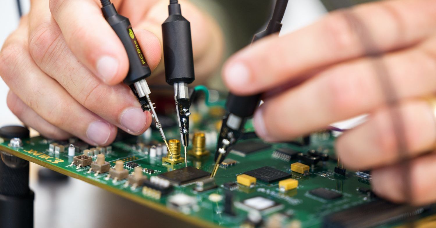
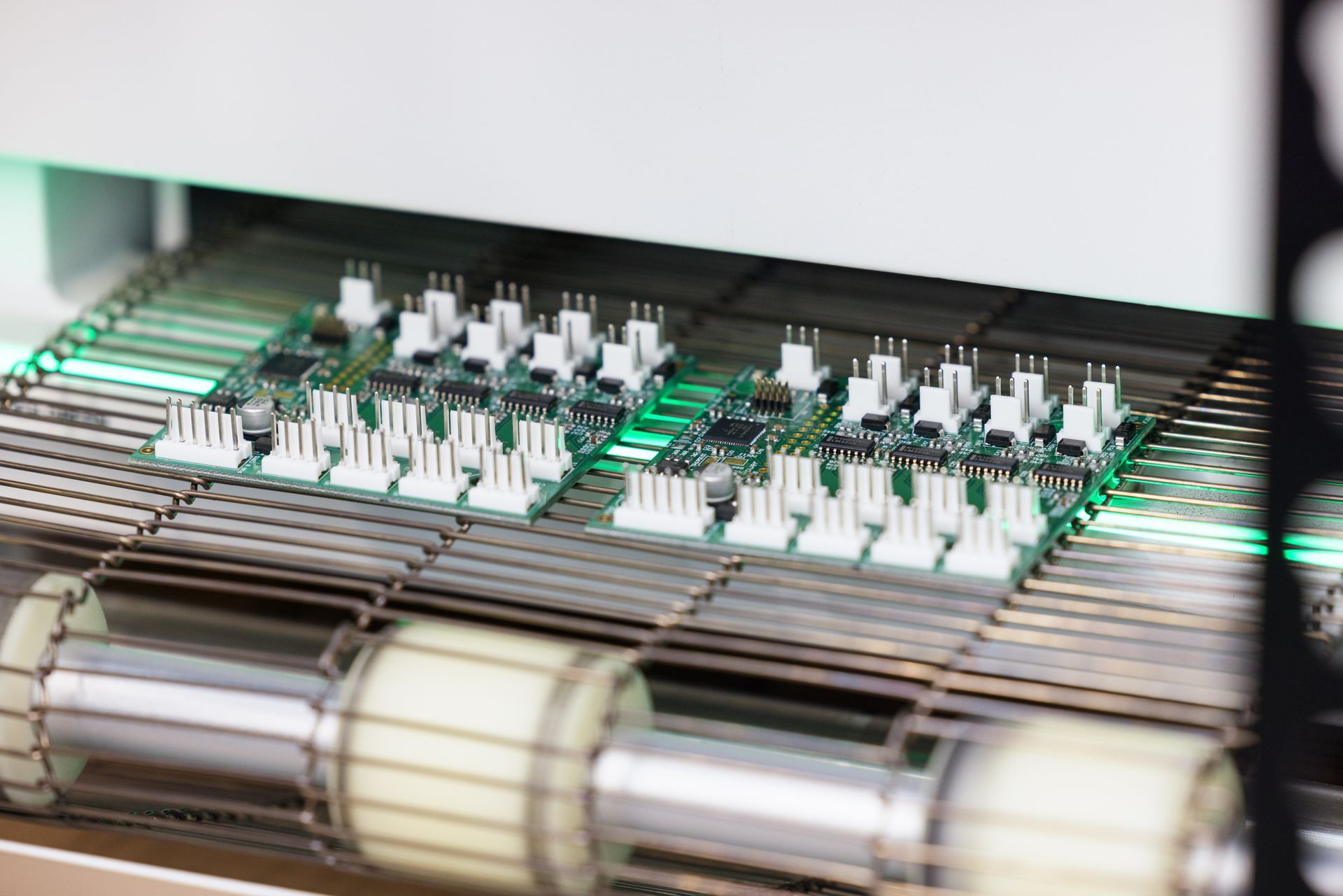
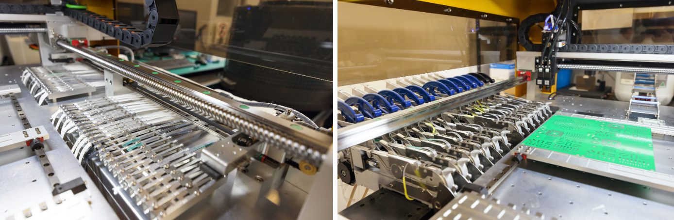
Prototyping & Testing
Once the schematics and PCBs are finalized, we can begin procuring prototypes. Typically, we budget for 2-3 spins, although more may be necessary for complex products.
The objective of Prototyping & Testing is to verify that the hardware design functions as intended and meets all specified requirements.
The first prototype spin provides the firmware team with their first opportunity to test their functionality on actual hardware, which often leads to valuable insights and learnings. This is why prototype runs are so important; despite thorough research and risk mitigation in Phase 1, due to the inherent complexity, it is highly likely that issues will arise during the prototyping phase. This should be expected.
By addressing these issues early through rigorous testing and validation, we ensure that the final product is reliable, functional, and meets all design criteria.
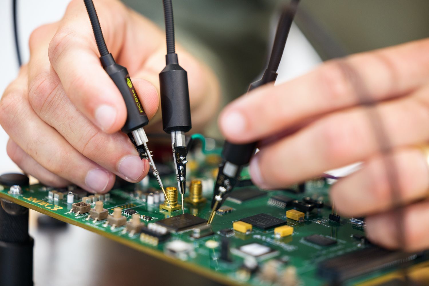
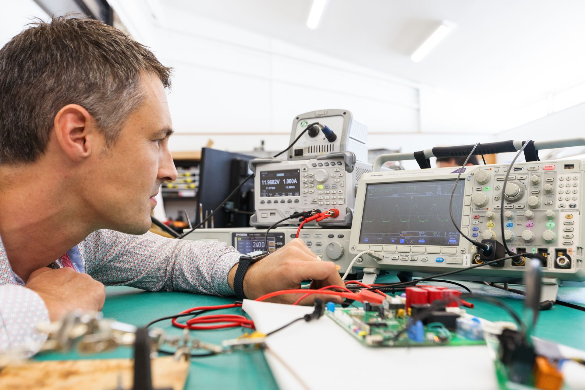
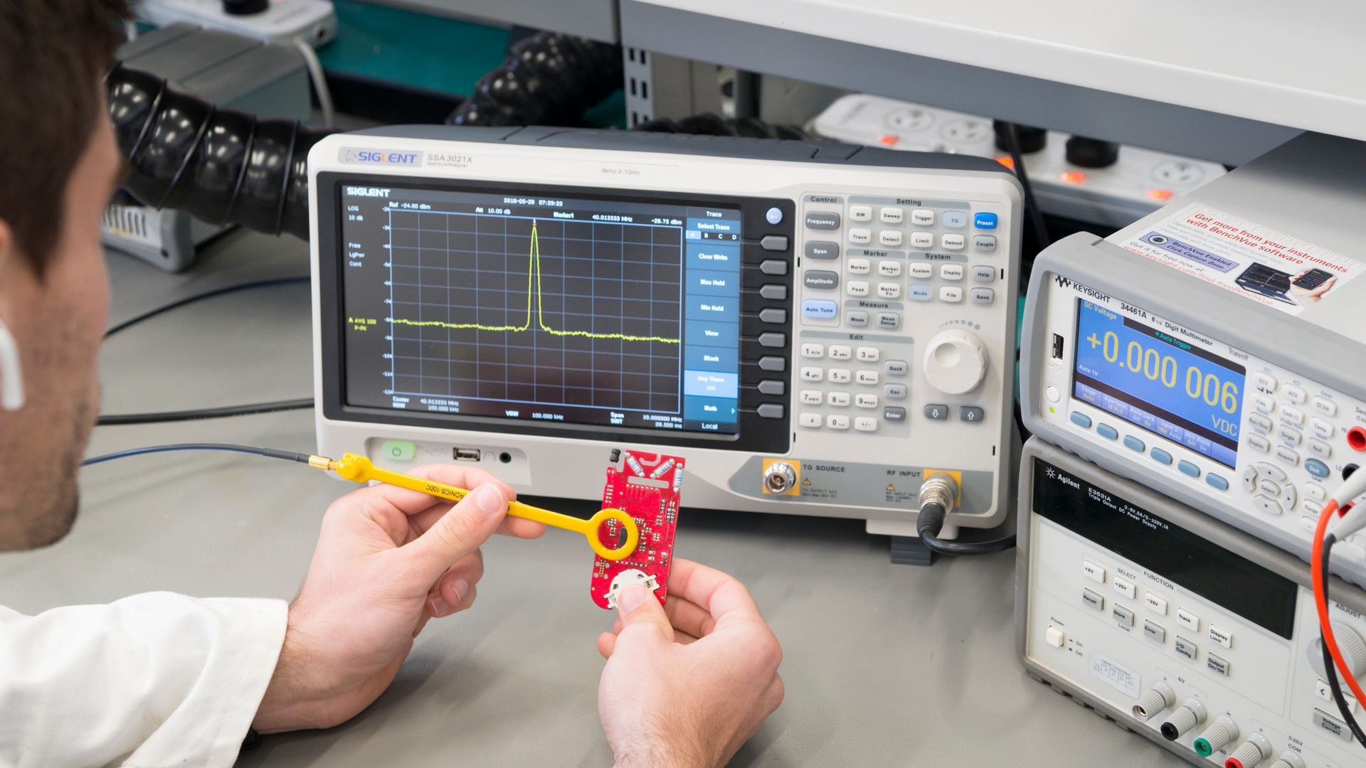
What is Tested & How?
NB: Depending on the project, only some of the following tests may be undertaken.
- Visual Inspection: Conduct a visual examination of the prototype to identify any obvious manufacturing defects.
- Power Supply Verification: Validate the power supply subsystem to ensure it delivers the correct voltages and currents without undue noise or instability.
- Thermals: Assess the thermal performance of the prototype by measuring key components and overall board temperatures under various operating conditions. Boards are run under a thermal camera looking for hot spots.
- Circuit Subsystems: Any parts of the circuit that can be tested without firmware will be.
- Electrical Extremes: Test all electronics over their full working range.
- EMC Pre-compliance Testing:
- TEM Cell: Used to measure approximate far-field radiated emissions from the PCB over a wide frequency spectrum by placing the PCB inside it. More convenient than far-field testing setups since it can all fit inside the EMC shielding tent.
- Near field probes: Used to measure specific frequencies at locations around the board to identify which areas are contributing to emissions.
- Far-field testing: measures the emissions using an antenna at a specific distance from the device e.g. 3 meters. The emissions levels are compared with limits from a compliance standard e.g EN55032.
The firmware development team is responsible for developing and integrating the software that controls the hardware. Firmware development has been running concurrently with hardware design and will likely continue throughout the entire process. Typically, the majority of the hardware's functionality requires firmware to be fully tested. The firmware engineers will work closely with the hardware team to verify and ensure all components function as intended. The detailed process and challenges of firmware development will be covered in more depth in a future blog.
Client Testing
After verifying most of the hardware, the client is expected to conduct thorough testing themselves. This is crucial as they can test the product in its intended use case. This often involves testing the hardware on actual equipment and environments where it will be used, as well as involving beta testers who can provide real-world feedback and identify any potential issues that may not have been evident during initial testing phases. To expedite this process, the product is often provided to the client before the firmware is fully implemented, allowing them to test a partially featured product. This ensures earlier detection of issues and provides ample time to address any long-term concerns.
What Tools Are Used?
Not every tool is necessary for every PCB project, but each has its specific applications and advantages. At Beta Solutions, we utilize a variety of tools including:
- Oscilloscope
- Multimeter
- Logic Analyser
- Signal analyser/ Network analyser
- Signal Generator
- IR Camera
Once all the hardware has been verified we can move into Phase 3 (Regulatory Compliance) or Phase 4 (Production Readiness) depending on the product. This move is generally marked by the formal approval of the customer acceptance testing results defined in phase 1. If all criteria are met, the product is deemed ready for stringent regulatory compliance checks and/or pre-production preparations.
Overview of Phases 3, 4, and 5
These phases will be explored in greater detail in future blog posts, covering specific challenges and best practices.
In Phase 3 - Regulatory Compliance, we ensure the product meets all required standards through rigorous testing and documentation to obtain compliance certificates. At times, this can be a considerable undertaking, often involving multiple iterations and reports to satisfy regulatory requirements.
Transitioning to Phase 4
- Production Readiness involves optimizing the design for large-scale manufacturing, conducting pilot production runs, and finalizing production documentation and pricing. This phase can be a significant investment depending on the setup costs involved. This is sometimes known as Non-recurring engineering (NRE).
Finally, Phase 5 - Volume Production transitions the design into mass manufacturing while focusing on quality assurance, ongoing support, and lifecycle management. For some customers, this might be 50 boards, for others it could be 100,000.
Why Choose Beta Solutions
Designing modern electronic hardware is a complex, multi-faceted endeavour that requires meticulous planning, deep expertise, and rigorous testing. At Beta Solutions, our time-tested process ensures that the complexities at each stage are managed effectively. This approach helps mitigate risks, meet regulatory standards, and ultimately bring robust, quality products to market.
As we have touched on in this blog, this process can be daunting, but with the right partner, it becomes manageable and highly rewarding.
If you're considering outsourcing your R&D to optimize your resources and focus on your core competencies, Beta Solutions are your ideal partners. See how you can get access to a dedicated team of experts here.